8 Semiconductor Manufacturing
Chapter Contents
20.1 Learning Objectives
20.2 Introduction
20.3 Clean Rooms
20.4 Silicon Processing
20.5 Lithography
20.6 Thin Films
20.7 Etch
20.8 Testing & Sorting / Packaging
20.9 Chapter Summary
20.10 References
20.1 Learning Objectives
By reading this chapter, you will learn the basic overview of Semiconductor Manufacturing, the clean room and its individual production areas including silicon production, clean rooms, lithography, thin films, etch, and sorting/testing. This chapter covers some of the basics while also digging into some of the advanced specifics of these semiconductor manufacturing processes.
20.2 Introduction
Microchips play a key role in every one of our lives. They are the thinking materials in every automated digital product including our phones, satellites, cars, computers. But what is a microchip? And what does that have to do with semiconductors? And why are they so complicated?
A semiconductor, usually silicon, is the material between an electrical conductor and insulator. It can be manipulated to be either one of those two with varying degrees of conductivity. A microchip is a thin micro-circuit built from the three of these components. For the use of this document, we will also use the term semiconductor in place of microchips. These microcircuits are like super highways for electrons, a grid of crisscrossing wires including resistors, transistors, capacitors, inductors and diodes that all control the flow of electrons. Together, this creates a central “brain” that can take in many inputs and spit out different outputs. As our technology advances, our capabilities for creating smaller and smaller microchips continues, allowing us to create more and more complex semiconductors in a smaller space. We can create more complex phones, vehicles, computer programs, AI, missile systems, power management systems, data collection procedures, robotics and microcontrollers, ect. This document will go over some of the complex manufacturing processes of semiconductor manufacturing including the clean rooms production happens, the creation of the silicon wafer, lithography and how it’s used to create the patterns needed for conductive and insulating layers, the deposition of layers, etching away specific regions, and the testing and sorting of final products.
20.3 Clean Room
Most of the processing sequence for integrated circuits must be carried out in a clean room, the ambiance of which is more like a hospital operating room than a production factory. Cleanliness is dictated by the microscopic feature sizes in an IC, the scale of which continues to decrease with each passing year. Figure 1.3 shows the trend in IC device feature size; also displayed in the same figure are common airborne particles that are potential contaminants in IC processing, These particles can cause defects in the integrated circuits, reducing yields and increasing costs.
A clean room provides protection from these contaminants. The air is purified to remove most of the particles from the processing environment; temperature and humidity are also controlled. A standard classification system is used to specify the cleanliness of a clean room. In the system, a number (in increments of ten) is used to indicate the quantity of particles of size 0.5 μm or greater in one cubic foot of air. Thus, a class 100 clean room must maintain a count of particles of size 0.5 μm or greater at less than 100/ft3.
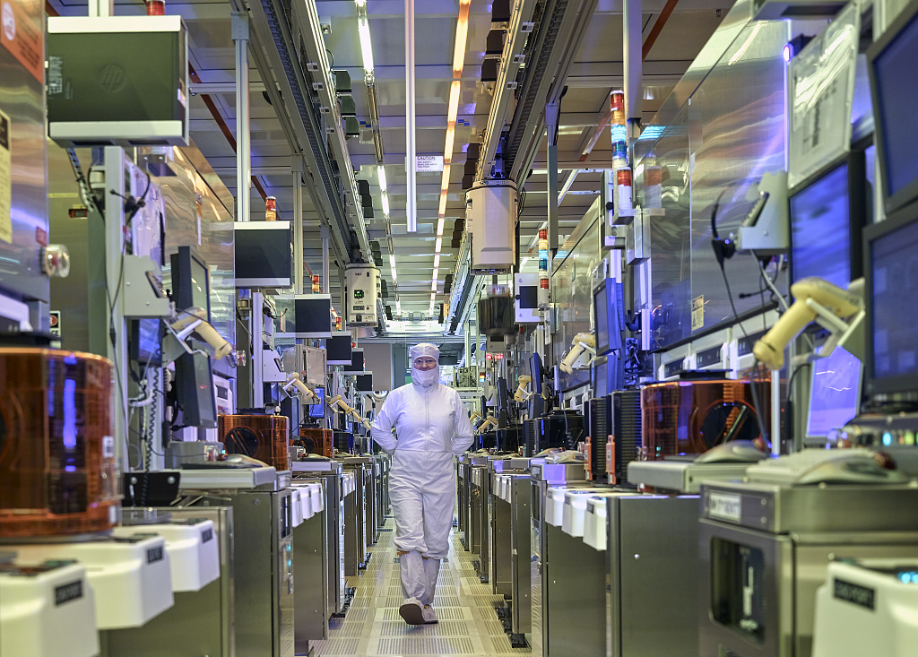
Modern processing requires class 10 clean rooms, which means that the number of particles of size equal to or greater than 0.5 μm is less than 10/ft3. The air in the clean room is air conditioned to a temperature of 21°C (70°F) and 45% relative humidity. The air is passed through a high-efficiency particulate air (HEPA) filter to capture particle contaminants.
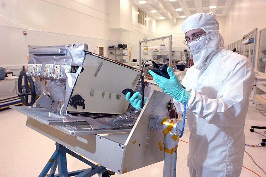
Humans are the biggest source of contaminants in IC processing; emanating from humans are bacteria, tobacco smoke, viruses, hair, and other particles. Human workers in IC processing areas are required to wear special clothing, generally consisting of white cloaks, gloves, and hair nets. Where extreme cleanliness is required, workers are completely encased in bunny suits. Processing equipment is a second major source of contaminants; machinery produces wear particles, oil, dirt, and similar contaminants. IC processing is usually accomplished in laminar-flow hooded work areas, which can be purified to greater levels of cleanliness than the general environment of the clean room. In addition to the very pure atmosphere provided by the clean room, the chemicals and water used in IC processing must be very clean and free of particles. Modern practice requires that chemicals and water be filtered prior to use.
20.4 Silicon Processing
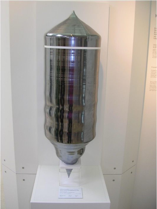
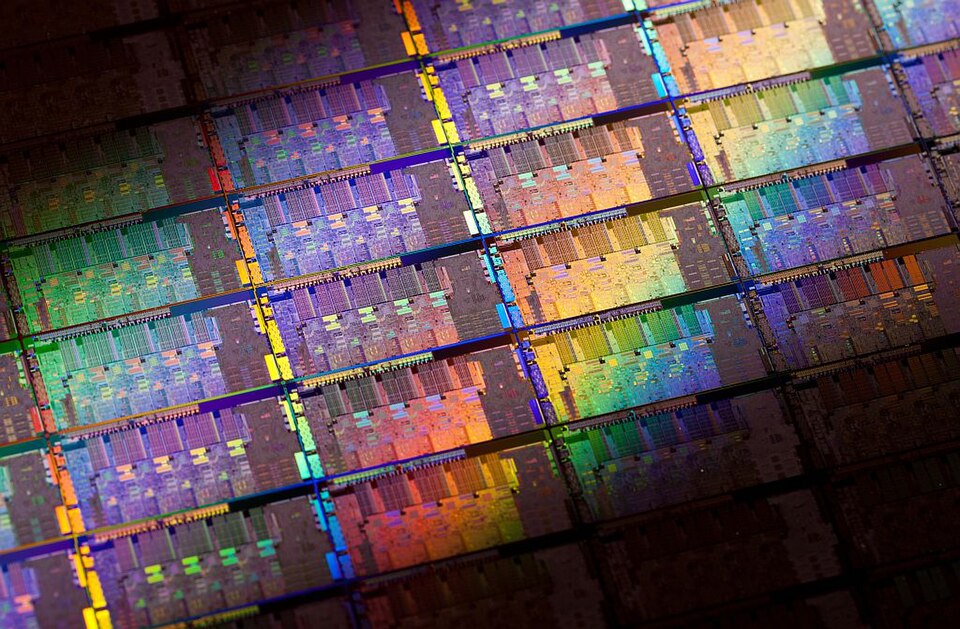
The sequence to fabricate a silicon-based IC chip begins with the processing of silicon. Briefly, silicon of very high purity is reduced in several steps from sand (silicon dioxide, SiO2). The silicon is grown from a melt into a large solid single crystal “log”, with typical length of 1-3 m (3-10 ft) and diameter up to 300 mm (12 in). The log, called a boule, is then sliced into thin wafers, which are disks of thickness equal to about 0.5 mm (0.020 in).
After suitable finishing and cleaning, the wafers are ready for the sequence of processes by which microscopic features of various chemistries will be created in their surface to form the electronic devices and their intra-connections. The sequence consists of several types of processes, most of them repeated many times. A total of 200 or so processing steps may be required to produce a modern IC. Basically, the objective in each step is to add, alter, or remove a layer of material in selected regions of the wafer surface. The layering steps in IC fabrication are sometimes referred to as the planar process, because the processing relies on the geometric form of the silicon wafer being a plane. 1 MOSFET stands for Metal-Oxide-Semiconductor Field-Effect Transistor. A transistor is a semiconductor device capable of performing various functions such as amplifying, controlling, or generating electrical signals. A field-effect transistor is one in which current flows between source and drain regions – through a channel, the flow depending on the application of voltage to the channel gate. A metal-oxide-semiconductor FET uses silicon dioxide to separate the channel and gate metallization. Packaging of an integrated circuit chip: (a) cutaway view showing the chip attached to a lead frame and encapsulated in a plastic enclosure, and (b) the package as it would appear to a user. This type of package is called a dual in-line package (DIP). Chip (die) Bonds (chip to leads) Lead frame (a) Overview of JC Processing 801 Molded plastic body (b) The processes by which the layers are added include thin film deposition techniques such as physical vapor deposition and chemical vapor deposition, and existing layers are altered by diffusion and ion implantation. Additional layer-forming techniques, such as thermal oxidation, are also employed. Layers are removed in selected regions by etching, using chemical etchants (usually acid solutions) and other more advanced technologies such as plasma etching.
The addition, alteration, and removal of layers must be done selectively; that is, only in certain extremely small regions of the wafer surface to create small device details. To distinguish which regions will be affected in each processing step, a procedure involving lithography is used. In this technique, masks are formed on the surface to protect certain areas and allow other areas to be exposed to the particular process (e.g:, film deposition, etching). By repeating the steps many times, exposing different areas in each step, the starting silicon wafer is gradually transformed into many integrated circuits.
Processing of the wafer is organized in such a way that many individual chip surfaces are formed on a single wafer. Since the wafer is round with diameters ranging from 150 to 300 mm (6-12 in), while the final chip may only be 12 mm (0.5 in) square, it is possible to produce hundreds of chips on a single wafer. At the conclusion of planar processing, each IC on the wafer is visually and functionally tested, the wafer is diced into individual chips, and each chip that passes the quality test is packaged.
Summarizing the preceding discussion, the production of silicon-based integrated circuits consists of the following stages: (1) Silicon processing, in which sand is reduced to very pure silicon and then shaped into wafers; (2) IC fabrication, consisting of multiple processing steps that add, alter, and remove thin layers in selected.
Two processes to create silicone wafers are mentioned here . The first is the Siemens process and the second is the Czachralski process. In the Siemens process Si is deposited onto a thin silicon rod by chemical vapor deposition. It is capable of producing silicon cylinders up to 200 mm (8 in) in diameter and 3 m (10 ft) in length. Siemens has been the dominant process in the industry since around 1970, but it suffers from several disadvantages: (1) high capital equipment cost; (2) high power consumption, (3) relatively low efficiency in yielding Si because of intermediate reaction products such as SiCl4; and ( 4) high labor cost because it is a batch process. The alternative process employs a fluidized-bed reactor rather than CVD, but similar reactions take place during the process. Use of the fluidized-bed process is expected to increase due to the following advantages over the Siemens method [6]: (1) higher Si yield in the product; (2) lower power consumption; and (3) continuous operation rather than batch. The silicon substrate for microelectronic chips must be made of a single crystal whose unit cell is oriented in a certain direction. The properties of the substrate and the way it is processed are both influenced by these factors. Accordingly, silicon used as the raw material in semiconductor device fabrication must not only be of ultra high purity, as in electronic grade silicon; it must also be prepared in the form of a single crystal and then cut in a direction that achieves the desired planar orientation. The crystal-growing process is covered here, while the next section details the cutting operation.
The most widely used crystal-growing method in the semiconductor industry is the Czachralski process, in which a single crystal ingot, called a boule, is pulled upward from a pool of molten silicon. The setup includes a furnace, a mechanical apparatus for pulling the boule, a vacuum system, and supporting controls. The furnace consists of a crucible and heating system contained in a vacuum chamber. The crucible is supported by a mechanism that permits rotation during the crystal-pulling procedure. Chunks of EGS are placed in the crucible and heated to a temperature slightly above the melting point of silicon: 1410°C (2570°F). Heating is by induction or resistance, the latter being used for large melt sizes.
To initiate crystal growing, a seed crystal of silicon is dipped into the molten pool and then withdrawn upward under carefully controlled conditions. At first the pulling rate (vertical velocity of the pulling apparatus) is relatively rapid, which causes a single crystal of silicon to solidify against the seed, forming a thin neck. The velocity is then reduced, causing the neck to grow into the desired larger diameter of the boule while maintaining its single crystal structure. In addition to pulling rate, rotation of the crucible and other process parameters are used to control boule size. Single-crystal ingots of diameter= 300 mm (12 in) and up to 3 m (10 ft) long are commonly produced for subsequent fabrication of microelectronic chips.
It is important to avoid contamination of the silicon during crystal growing, since contaminants, even in small amounts, can dramatically alter the electrical properties of Si. To minimize unwanted reactions with silicon and the introduction of contaminants at the elevated temperatures of crystal growing, the procedure is carried out either in an inert gas (argon or helium) or a vacuum.
20.5 Lithography
An IC consists of many microscopic regions on the wafer surface that make up the transistors, other devices, and intra-connections in the circuit design. In the planar process, the regions are fabricated by a sequence of steps, each step adding another layer to selected areas of the surface. The form of each layer is determined by a geometric pattern representing circuit design information that is transferred to the wafer surface by a procedure known as lithography-basically the same procedure used by artists and printers for centuries.
Several lithographic technologies are used in semiconductor processing: (1) photolithography, (2) electron lithography, (3) X-ray lithography, and (4) ion lithography. As their names indicate, the differences are in the type of radiation used to transfer the mask pattern to the surface by exposing the photoresist. The traditional technique is photolithography, and most of our discussion will be directed at this topic. The reader may recall that photolithography is used in some chemical machining processes.
Photolithography, also known as optical lithography, uses light radiation to expose a coating of photoresist on the surface of the silicon wafer; a mask containing the required geometric pattern for each layer separates the light source from the wafer, so that only the portions of the photoresist not blocked by the mask are exposed. The mask consists of a flat plate of transparent glass onto which a thin film of an opaque substance has been deposited in certain areas to form the desired pattern. Thickness of the glass plate is around 2 mm (0.080 in), while the deposited film is only a few μ.m thick-for some film materials, less than a μ.m. The mask itself is fabricated by lithography, the pattern being based on circuit design data, usually in the form of digital output from the CAD system used by the circuit designer.
A photoresist is an organic polymer that is sensitive to light radiation in a certain wavelength range; the sensitivity causes either an increase or decrease in solubility of the polymer to certain chemicals. Typical practice in semiconductor processing is to use photoresists that are sensitive to ultraviolet light. UV light has a short wavelength compared to visible light, permitting sharper imaging of microscopic circuit details on the wafer surface. It also permits the fabrication and photoresist areas in the plant to be illuminated at low light levels outside the UV band.
Two types of photoresists are available: positive and negative. A positive resist becomes more soluble in developing solutions after exposure to light. A negative resist becomes less soluble ( the polymer cross-links and hardens) when exposed to light. The principal advantage of the positive resist is better resolution. The negative resists have better adhesion to SiO2 and metal surfaces, good etch resistance, high sensitivity, and low cost.
Exposure Techniques The resists are exposed through the mask by one of three exposure techniques: (a) contact printing, (b) proximity printing, and (c) projection printing. In contact printing, the mask is pressed against the resist coating during exposure. This results in high resolution of the pattern onto the wafer surface; an important disadvantage is that physical contact with the wafers gradually wears out the mask. In proximity printing, the mask is separated from the resist coating by a distance of 10-25 μm (0.0004-0.001 in). This eliminates mask wear, but resolution of the image is slightly reduced. Projection printing involves the use of a high-quality lens (or mirror) system to project the image through the mask onto the wafer. This has become the preferred technique because it is noncontact (thus, no mask wear), and the mask pattern can be reduced through optical projection to obtain high resolution.
20.6 Thin Films
Oxidation of the silicon wafer may be performed multiple times during fabrication of an integrated circuit. Silicon dioxide (SiO2) is an insulator, contrasted with the semiconducting properties of Si. The ease with which a thin film of SiO2 can be produced on the surface of a silicon wafer is one of the attractive features of silicon as a semiconductor material. Silicon dioxide serves a number of important functions in IC fabrication:
- It is used as a mask to prevent diffusion or ion implantation of dopants into silicon
- It can be used to isolate devices in the circuit;
- It is a critical component in certain types of MOS devices; and
- It provides electrical insulation between levels in multilevel metallization systems.
Several processes are used to form SiO2 in semiconductor manufacturing, depending on when during chip fabrication the oxide must be added, The most common process is thermal oxidation, appropriate for growing SiO2 films on silicon substrates. In thermal oxidation, the wafer is exposed to an oxidizing atmosphere at elevated temperature; either oxygen or steam atmospheres are used. Typical temperatures used in thermal oxidation of silicon range from 900° to 1300°C (1650′-2350″F). By controlling temperature and time, oxide films of predictable thickness can be obtained. Films produced by thermal oxidation possess an amorphous structure, good uniformity, and low incidence of pinholes and similar defects.
When a silicon dioxide film must be applied to surfaces other than silicon, then direct thermal oxidation is not appropriate. An alternative process must be used, such as chemical vapor deposition.
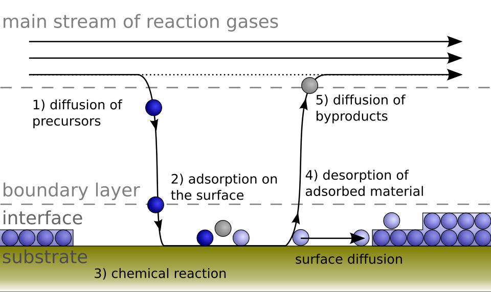
Chemical vapor deposition (CVD) involves growth of a thin film on the surface of a heated substrate by chemical reactions or decomposition of gases. CVD is widely used in the processing of integrated circuit wafers to add layers of silicon dioxide, silicon nitride (Si3N4), and silicon. Plasma-enhanced CVD is often used because it permits the reactions to take place at lower temperatures.
Typical CVD Reactions in lC Fabrication In the case of silicon dioxide, if the surface of the wafer is only silicon (e.g., at the start of IC fabrication), then thermal oxidation is the appropriate process by which to form a layer of SiO2. If the oxide layer must be grown over materials other than silicon, such as aluminum or silicon nitride, then some alternative techniques must be used, such as CVD. Chemical vapor deposition of
SiO2 is accomplished by reacting a silicon compound such as silane (SiH,) with oxygen onto a heated substrate. The reaction is carried out at around 425°C (800°F). The density of the silicon dioxide film and its bonding to the substrate is generally poorer than that achieved by thermal oxidation. Consequently, CVD is used only when the preferred process is not feasible-when the substrate surface is not silicon, or when the high temperatures used in thermal oxidation cannot be tolerated. CVD can be used to deposit layers of doped Si 0 2, such as phosphorus-doped silicon dioxide (called P-glass).
Silicon nitride is used as a masking layer during oxidation of silicon. ShN4 has a low oxidation rate compared to Si, so a nitride mask can be used to prevent oxidation in coated areas on the silicon surface. Silicon nitride is also used as a passivation layer (protecting against sodium diffusion and moisture).
Plasma-enhanced CVD is also used for basically the same coating reaction, the advantage being that it can be performed at much lower temperatures-around 300°C (600°F).
Polycrystalline silicon (called polysilicon to distinguish it from silicon having a single crystal structure such as the boule and wafer) has a number of uses in IC fabrication, including conducting material for leads, gate electrodes in MOS devices, and contact material in shallow junction devices. Chemical vapor deposition to coat polysilicon onto a wafer involves reduction of silane at temperatures around 600°C (1100F).
Etch
All of the preceding processes in this section involve addition of material to the wafer surface, either in the form of a thin film or the doping of the surface with an impurity clement. Certain steps in IC manufacturing require material removal from the surface; this is accomplished by etching away the unwanted material. Etching is usually done selectively, by coating surface areas that are to be protected and leaving other areas exposed for etching. The coating may be an etch-resistant photoresist, or it may be a previously applied layer of material such as silicon dioxide. We briefly encountered etching in our description of photolithography.
There are two main categories of etching process in semiconductor processing: wet chemical etching and dry plasma etching.
Wet Chemical Etching
Wet chemical etching is the older of the two processes and is easier to use. However, there are certain disadvantages that have resulted in growing use of dry plasma etching. Wet Chemical Etching Wet chemical etching involves the use of an aqueous solution, usually an acid, to etch away a target material. The etching solution is selected because it chemically attacks the specific material to be removed and not the protective layer used as a mask.
Dry Plasma Etching
Dry etching is a technique of transferring a pattern into a material using reactive gases. Typically this process involves generating a plasma in a process reactor using RF energy to ionize the reactive gases. Plasmas are very complex and have numerous different reactions happening in the plasma simultaneously. These reactions form ions, neutrals, and radicals in the plasma that are then accelerated to the surface of the material by an electric field. The electric field is formed between the plasma and the material to be etched. Dry etching is a more complex technique that may or may not have good selectivity between different materials which can be a drawback. However, the major advantage is that dry etching is typically very anisotropic in nature which allows for very reproducible etch characteristics (Penn State Nanofabrication Lab).
20.8 Testing & Sorting / Packaging
The packaging of an IC chip in manufacturing can be divided into the following steps:
- Wafer testing,
- Chip separation,
- Die bonding,
- Wire bonding, and
- Package sealing. After packaging, a final functional test is performed on each packaged IC.
20.8.1 Wafer Testing
Current semiconductor processing techniques provide several hundred individual ICs per wafer. It is convenient to perform certain functional tests on the I Cs while they are still together on the wafer-before chip separation. Testing is accomplished by computer-controlled test equipment that uses a set of needle probes configured to match the connecting pads on the surface of the chip; multiprobe is the term used for this testing procedure. When the probes contact the pads, a series of DC tests are carried out to indicate short circuits and other faults; this is followed by a functional test of the IC. Chips that fail the test are marked with an ink dot; these defects are not packaged. Each IC is positioned in its turn beneath the probes for testing, using a high precision x-y table to index the wafer from one chip site to the next. Lower performing chips can be sold as a weaker chip, therefore reducing waste as scrapped chips that still perform can still be used.
20.8.2 Chip Separation
The next step after testing is to cut the wafer into individual chips (dice). A thin diamond-impregnated saw blade is used to perform the cutting operation. The sawing machine is highly automated and its alignment with the “streets” between circuits is very accurate. The wafer is attached to a piece of adhesive tape that is mounted in a frame. The adhesive tape holds the individual chips in place during and after sawing; the frame is a convenience in subsequent handling of the chips. Chips with ink dots are now discarded.
20.8.3 Die Bonding
The individual chips must next be attached to their individual packages, a procedure called die bonding. Owing to the miniature size of the chips, automated handling systems are used to pick the separated chips from the tape frame and place them for die bonding. Various techniques have been developed to bond the chip to the packaging substrate; we describe two methods that seem to be the most important today: eutectic die bonding and epoxy die bonding. Eutectic die bonding, used for ceramic packages, consists of the following steps: (1) a thin film of gold is deposited on the bottom surface of the chip; (2) the base of the ceramic package is heated to a temperature above 370°C (698°F), the eutectic temperature of the Au-Si system; and (3) the chip is bonded to the metallization pattern on the heated base. In epoxy die bonding, used for plastic VLSI packaging, a small amount of epoxy is dispensed on the package base (the lead frame), and the chip is positioned on the epoxy; the epoxy is then cured, bonding the chip to the surface.
20.8.3 Wire Bonding
After the die is bonded to the package, electrical connections are made between the contact pads on the chip surface and the package leads. The connections are generally made using small-diameter wires of aluminum or gold. Typical wire diameters for aluminum are 0.05 mm (0.002 in), and gold wire diameters are about half that diameter (Au has higher electrical conductivity than Al, but is more expensive). Aluminum wires are bonded by ultrasonic bonding, while gold wires are bonded by thermocompression, thermosonic, or ultrasonic means. Ultrasonic bonding uses ultrasonic energy to weld the wire to the pad surface. Thermocompression bonding involves heating the end of the wire to form a molten ball, and then the ball is pressed into the pad to form the bond. Thermosonic bonding combines ultrasonic and thermal energies to form the bond. Automatic wire bonding machines are used to perform these operations at rates up to 200 bonds per minute.
20.8.4 Package Sealing
As mentioned above, the two common packaging materials are ceramic and plastic. The processing methods are different for the two materials. Ceramic packages are made from a dispersion of ceramic powder (AhO3 is most common) in a liquid binder (e.g., polymer and solvent). The mix is first formed into thin sheets and dried, and then cut to size. Holes are punched for interconnections. The required wiring paths are •then fabricated onto each sheet, and metal is filled into the holes. The sheets are then laminated by pressing and sintering to form a monolithic ( single stone) body.
An alternative and lower cost ceramic package involves sealing of the IC chip between two ceramic plates using refractory glass, glass whose melting point is around 400°C (750°F). This provides hermetic sealing but is not capable of the complexity of the more Conventional ceramic package. The technique goes by the name CERDIP (for glass-sealed ceramic D!Ps) and CERQUADs for the corresponding quad packs.
Two types of plastic package are available, postmolded and premolded. In postmolded packages, an epoxy thermosetting plastic is transfer molded around the assembled chip and lead frame (after wire bonding), in effect transforming the pieces into one solid body. However, the molding process can be harsh on the delicate bond wires, and premolded packages are an alternative. In premolded packaging, an enclosure base is molded prior to encapsulation and then the chip and lead frame are connected to it,adding a solid lid or other material to provide protection. The extra assembly steps cause this production method to be more costly than postmolding.
20.8.5 Final Testing
Upon completion of the packaging sequence, each IC must undergo a final test, the purpose of which is (I) to determine which units, if any, have been damaged during packaging, and (2) to measure performance characteristics of each device. Burn-in test procedures sometimes include elevated temperature testing, in which the packaged IC is placed in an oven at temperatures around 125°C (250°F) for 24 hours and then tested. A device that fails such a test would have been likely to have failed early curing service. If the device is intended for environments where wide temperature variations occur, a temperature cycle test is appropriate. This test subjects each device to a series of temperature reversals, between values around -50°C (-60°F) on the lower side and 125°C (250°F) on the upper side. Additional tests for devices requiring high reliability might include mechanical vibration tests and hermetic (leak) tests.
20.9 Chapter Summary
In summary, we have gone over the main processes that make up semiconductor manufacturing. We’ve gone over the production of silicon and the wafer, Clean rooms, Lithography, Chemical vapor deposition, Etch, and Sorting. These advanced processes make a microchip and are becoming increasingly valuable in today’s world. The economy of this major resource is vast and includes huge amounts of very skilled workers.
20.10 References
Chao, T. S. Introduction to semiconductor manufacturing technology. New Jersey: Prentice Hall, 2000.
Groover, Mikell P. Fundamentals of Modern Manufacturing: Materials, Processes, and Systems. J. Wiley & Sons, 2007.
May, Gary S., and Costas J. Spanos. Fundamentals of Semiconductor Manufacturing and Process Control. IEEE ; Wiley-Interscience, 2006.
Nishi, Yoshio, and Robert Doering. Handbook of Semiconductor Manufacturing Technology. Marcel Dekker, 2000.
“Semiconductor Front-End Process Episode 5.” SK Hynix Newsroom –, 5 Dec. 2023, news.skhynix.com/semiconductor-front-end-process-episode-5/.
“Dry Etch | Materials Research Institute.” psu.edu, 2025, www.mri.psu.edu/nanofabrication-lab/capabilities/etching/dry-etch. Accessed 22 Dec. 2025.
Media Attributions
- Intel 2nd Generation Core microprocessor codenamed Sandy Bridge Wafer © Intel Free Press is licensed under a CC BY-SA (Attribution ShareAlike) license
- Clean Room (23928923558) © cuboulder is licensed under a CC0 (Creative Commons Zero) license
- service-pnp-highsm-55000-55093v © Highsmith (Carol M.) is licensed under a Public Domain license
- Silicon single crystal © Massimiliano Lincetto is licensed under a CC BY-SA (Attribution ShareAlike) license
- Sequence during CVD (en) © User:Cepheiden is licensed under a CC BY-SA (Attribution ShareAlike) license
